NOC: Next generation system architecture
This section gives an overview of the various aspects related to Networks-On-Chip (NOC). Covering the origination and motivation of the NOC paradigm as well as technical aspects of the layered system approach. Lastly, remarks on the design flow are depicted, like for instance modeling, verification or design space Exploration.
- Origination
Development of semiconductor technology and system design that motivates a paradigm shift to Networks-On-Chip
- Fundamentals
Brief introduction to the architecture, mode of operation and characteristics of NOCs
- Signal transmission
Operation of the physical layer (1) and the data link layer (2) to transmit data between neighboring components
- Networking
Abstract transmission of messages in a communication infrastructure with the networking layer (3) and the transport layer (4)
- Applications & OS
User applications and system control with an appropriate operating system in the application layer (7)
- Design flow
Necessary worksteps during development of NOC based architectures
Development of technology
The fundamental component of microelectronics is the transistor which was introduced commercially in the sixties. Since then, the continuous reduction of transistor dimensions has been the driving force of the semiconductor industry to achieve ever higher logic complexity and increased performance, at reduced costs per transistor. This development is about to continue and the International Technology Roadmap for Semiconductors (ITRS) predicts by the end of this decade up to several billion transistors on a single chip with feature sizes below 50 nm, operating at frequencies in the 10 GHz range.
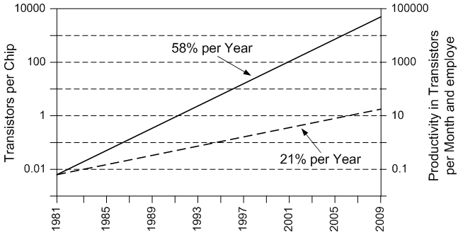
Figure 1 depicts the exponential growth of transistors per chip since the introduction of the personal computer (PC) in 1981. However, the scaling and growth in complexity does not affect all properties likewise which causes new problems and challenges that need to be faced at various abstraction levels and in different design steps.
In the following a few examples are given which illustrate some of the problems connected to nanotechnology. Power consumption has been increasing similarly to the integration density and has reached unacceptable levels. Thereby, leakage and subthreshold currents, which have formerly been of rather small impact, will soon dominate the overall power consumption. This does not just endanger the runtime of mobile devices but also further increases the power density to prohibitive levels. Moreover, the wire delay, especially that of global wires in higher metal layers, does not scale well and will determine the system performance. Hence, in combination with large chip size and high frequencies, the implementation of synchronous designs will be very hard and demands additional area and power consumption. The clock generation and distribution will thereby limit the area of synchronous modules within integrated circuits to an acceptable size.
However, such issues can also be recognized on the architectural level and during implementation. One example is the memory-bottleneck which describes the fact that it takes up to several hundred clock cycles to access the memory while computation stalls. Admittedly, this effect can be mitigated by deploying multi-level cache, run-ahead execution or adaptive memory scheduling, but again, only at the price of extra area and power dissipation. Finally, the productivity for designing integrated circuits can not keep up with the rising logic complexity which is generally described as the design-productivity-gap (see figure 1). This leads to increasing costs and time to market as well as to degradation of product quality.
There is a large number of further issues ─ e.g. electromigration, crosstalk, soft errors, parameter variations, verification, scalability, re-use ─ that can not be covered briefly but need to be considered thoroughly during system design.
..: Recapitulating, advancements on all design and production levels or even new design methodologies are needed to overcome the ongoing and future expected issues of nanotechnology :..
Basic composition of an NoC
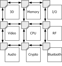
Networks-on-Chip (NoC) have been suggested as an option to cope with issues of conventional bus-based or point-to-point connected systems in current and future technologies. An NoC consists of miscellaneous independent resources ─ e.g. general purpose processors, memories, I/Os or any kind of intellectual properties (IPs) ─ which might be implemented with different voltages, frequencies or even diverse technologies. The resources are connected to a global network by an interface that encapsulates the communication- and computation-structures from another (see figure 1). The chosen interface allows to exchange different modules or to incorporate resources from vendors without influencing other resources and their internal behavior. The network by itself is composed of links as well as routers and features services such as guarantees for bandwidth or latency that enable the resources to communicate with each other.
Such an approach denotes a considerable shift from computation-centric to communication-centric system design. Though, extensive investigations to implement and to verify the new design methodology are required. To this day, a lot of effort has been put into designing the fundamental components of NoC, focusing mostly on functionality and performance. For instance repeater, booster and current sensing techniques have been suggested for signal transmission, coding and error correction schemes have been analyzed as well as virtual channel routers have been integrated in various topologies (e.g. mesh, torus, fat-tree, irregular) applying diverse routing schemes (e.g. dimension-ordered, adaptive, deflective). First prototypes of functional NoC implementations have also been presented with a relatively small number of resources for testing purposes or specific applications, mostly motivated by the domain of mobile and wireless consumer products. Such chips have pointed out the functionality of NoC in principle, its connected benefits and existing challenges.
..: Characteristic features of NoC are concurrency and modularity :..
Multi-hop communication
To communicate messages between distant resources requires using the network and transport layer to transmit the information via different intermediate nodes (several hops). Thereto, three major fields have to be considered and suitable solutions have to be chosen.
The first one is the type of switching scheme that is to be used in the on-chip network because the physical links are limited in size (e.g. 32, 64, 256 bit wide) and cannot transmit a large message at once. Thus, the switching scheme describes how a large message is segmented in packets and sent via intermediate nodes to its destination. Possible and well-known approaches are wormhole switching, virtual-cut-through and store-and-forward whereas the former is the most widespread solution due to little required buffer space ─ this is very closely related to little power consumption.
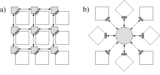
The second consideration affects the topology, i.e. how various computational resources are distributed in the network and how they are interconnected to each other. Most current publications use mesh networks ─ i.e. a 2-dimensional regular grid ─ due to its regularity and simplicity. However, this seems not appropriate for embedded systems with heterogeneous resources and requirements. A wide range of other topologies exists and it is also being investigated and used in the different application domains. Figure 1 depicts two simple examples of a mesh and a star topology. Further topologies are generally denoted as torus, fat-tree, ring, n-dimensional cube and more as well as heterogeneous topologies for application specific systems.
Lastly, an applicable routing algorithm has to be chosen that determines on which path (s) packets are transmitted to reach their destination. Such algorithms can be grouped by different characteristics whereas deterministic/adaptive and source-based/distributed are the two most common approaches. The simplest approach is the dimension-ordered routing or also called XY-routing. Thereby, a packet is routed in the X-dimension first until it has reached the final column of its destination. Then, the packet is solely routed in the Y-dimension.
Routing algorithms affect many - often contradicting - parameters and have to be chosen and investigated thoroughly (e.g. throughput, power consumption, area, latency, quality-of-service, reliability, congestion/deadlock). A priori knowledge of the traffic patterns and the target application helps significantly to achieve the design constraints.
The simple description of a router can be dowloaded here.
A few remarks describing the router-packet:
- Description given in VHDL
- XY-routing
- Wormhole switching
- Every flit is acknowledged
- Simple mesh scenario is also provided
..: The three main keywords to transmit packets to distant destinations in a network are switching scheme, topology and routing algorithm :..
HW/SW Codesgin
The upper layers 5 to 7 represent the application oriented layers. They are mostly closely coupled with each other.
Thereby, user applications can either be realized in hardware as hard-wired IP cores or be implemented in software on embedded general purpose processor cores that are connected to the NOC infrastructure. Mixed solutions and pure Multiprocessor SoCs (MPSoCs) are feasible as well.
Appropriate operating systems might run on embedded microprocessors, which do system surveillance, control, and management.
Bridge modules similar to network interface cards translate between the NOC interface and the application specific interfaces of the respective IP cores. Mostly, they offer features for end-to-end flow control and quality-of-service as well.
You can find some examples under the menu entry Projects, for instance hard-wired IP cores with focus on network packet processing and an adapted NOC operating and management system.
Semi-automated development
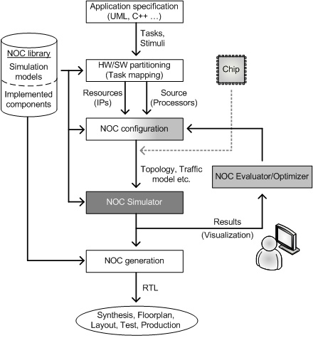
An automated design flow is needed to increase productivity and to allow the design of complex integrated circuits. Hereby, the NoC design flow should support all steps from system specification, via design development and optimization to the final mask generation for production. The investigation and implementation of such a flow requires tremendous efforts but includes parts that are not solely connected to NOC. The only exception is the NOC simulator that has to be developed to allow an overall system characterization. Thereto, extracted values of power consumption and latency as well as topology and traffic model are required as inputs.
The possible integration of a NOC simulator into a design flow is shown in figure 1. Iterative loops and more detailed steps (e.g. test, netlister, verification) are omitted for simplification. Besides the need for development, the simulator also offers the chance to investigate further open issues in the long-run. For instance, design space exploration for specific applications or domains.
However, to efficiently implement applications for a given NoC architecture, appropriate programming models are necessary to exploit specific properties like the parallel structure of resources or distributed memory. If such models and programs exist, it will be necessary to determine how programs can be mapped onto a given NoC architecture. This so called application mapping can occur both during development phase and during online operation and requires consideration of communication-computation trade-offs, power issues, quality of service requirements or thermal characteristics. Because sporadic errors will be unavoidable and malfunction of resources will have to be dealt with, testing and verification also needs to be considered at some stage. This will allow static adaptation or even online self-healing and can also increase yield and reliability of large integrated circuits. Finally, it demands for appropriate metrics and benchmarks to assess own solutions or to compare achieved results within the research community.
..: Automated design flow is required to allow the development of complex integrated circuits, increase productivity and reduce costs :..